
Studies of Initial Growth of GaN on InN Buffer Layers
Student: Alaa Alnami
Degree: M.S., December 2019
Major Professor: Dr. Morgan Ware
Research Area(s):
Microelectronics
Nanoscience & Engineering
Background/Relevance
- III-Nitride materials, such as GaN and InN, have recently attracted much attention for applications in microelectronics and optoelectronics.
- New devices may be realized using GaN growth on InN, however, attempts to make high quality interfaces have had limited success.
- Growth and formation of this interface needs to be improved.
Innovation
-
GaN/InN MBE growth with different growth conditions and different GaN thicknesses; studying the quality of the grown samples by AFM, XRD, SEM, PL, EDX, and Raman.
Approach
- Studying and optimizing the surface of GaN grown on InN.
- Growing different structures with variable growth temperature.
- Growing different GaN layer thickness by molecular beam epitaxy (MBE).
- Performing the structural characterization by AFM, XRD, SEM, PL, EDX and Raman.
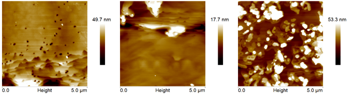
Key Results
- AFM images of InN layers grown on GaN/sapphire substrate.
- The growth condition is 400 ˚C with thickness of 1000 nm.
- AFM image of GaN layer after the growth with thickness of 50 nm grown at high temperature.
Conclusions
- Growing a 10 nm GaN at low temperature and then growing a 50 nm GaN at high temperature on InN layer did not prevent the evaporation of InN layer at high temperature.
- GaN on InN was successfully grown at 400 C˚, and InGaN alloys was found between the two layers. However, the surface of GaN was very rough at this low temperature growth.
Future Work
-
TEM needs to be done to investigate the quality and structure of the interface. Also, a variety of low temperature growths of GaN to enhance the surface morphology and structure quality are needed.