Defect Characterization of HVPE GaN Substrates
Student: Alaa Kawagy
Degree: M.S., May 2019
Major Professor: Dr. Morgan Ware
Research Area(s):
Nanoscience & Engineering
Microelectronics
Background/Relevance
- Gallium nitride (GaN) is a semiconductor material that has desirable physical properties such as wide bandgap energy, and large breakdown field making it useful for high-performance semiconductor devices for high efficiency.
- Recent availability of low cost substrates grown by HVPE creates opportunities for growth in research and production, however there are large scale macro defects on these substrates.
Innovation
-
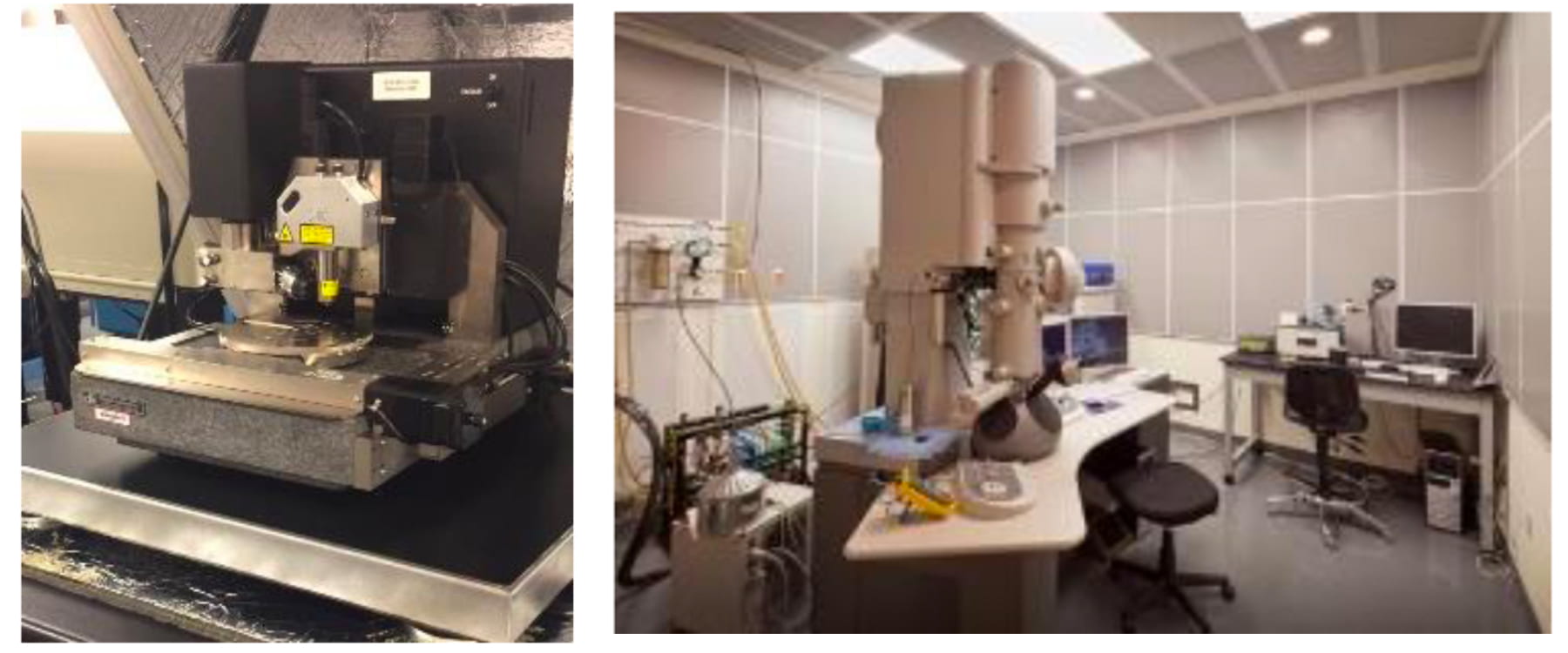
GaN substrates will be characterized by different microscopes. The GaN substrate and buffer will be characterized by TEM.
Approach
- Studying the defects of HVPE GaN substrates.
- Studying the substrates by using atomic force microscopy (AFM).
- Studying the substrate structural properties by X-ray diffraction to know the dislocation densities.
- Characterize the substrate by optical microscope and SEM.
- Studying the growth of GaN buffers on the GaN substrate by transmission electron microscopy (TEM) at 265Kx to 340Kx magnification.

Key Results
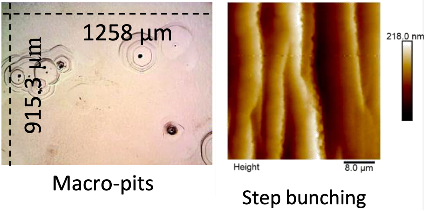
- Large steps and small pits were detected in unintentionally doped GaN substrates.
- Macro-pits were detected in semi-insulating GaN substrates.
- GaN substrates suffer from screw and mixed dislocations.
- Optical properties of GaN are not affected by defects in the substrates
- GaN buffer layer on GaN substrates has the same defect that found in the substrates.

Conclusions
- GaN suffers from small and large defect densities.
- The received GaN substrates vary in defect density, and some of them are good and some of them are not.
- The defects in the substrates affect the subsequent growth.
Future Work
- Using Photoluminescence for studying the GaN substrates.
- Using TEM for studying the grown GaN buffers on the GaN substrates.
