Ohmic Contact for SiC CMOS Devices
Student: Anthony Di Mauro
Major Professor: Dr. Radwan Al Faouri
Research Area(s):
Microelectronics-Photonic Materials & Devices
Energy Materials & Devices
Background/Relevance
- High demand for high temperature and high performance integrated circuits (Ics) which can replace traditional Si ICs and pack more processing power.
- SiC has a great outlook for automobile integration, power grid infrastructure, and other applications in harsh environments.
- CMOS devices will prove more useful with robust ICs that can maintain integrity in extreme conditions for lengthy durations.
Innovation
- Utilizing multiple materials, an ohmic contact can be formed for both n- and p-type semiconductor materials, which means better switching speeds and higher efficiency processes.
Approach
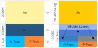
- Multilayered Silicide allows for high-quality diffusion of material between SiC-metal interface.
- RTA must be between 900-1100°C with inert gases for bulk layers.
- Short, high-temp annealing allows for small steps in band energy between the substrate and contact.

Key Results
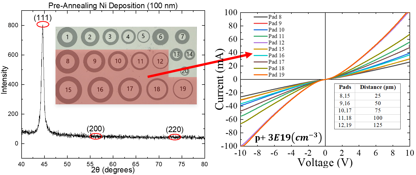
- Using a Circular Transfer Line Measurement (CTLM) device, the IV characteristics show linear behavior for P+ devices with a specific contact resistivity of 1.9E-3(Ω⋅cm2 ).

Conclusions
- A compromise will have to be made between the doping concentration for both types of materials and the quality of the contact which will affect the specific contact resistivity.
- The ohmic behavior of the p+ sample indicates less of a barrier between the substrate and the metal-contact interface.
- Without annealing the contact after deposition, no silicide was able to form, leading to a higher resistance.
- N-type samples will require higher doping concentrations for simultaneous ohmic contacts with this approach.
