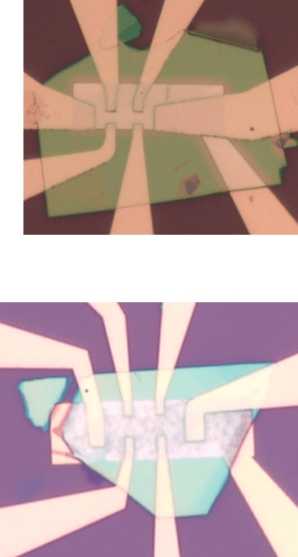
Electrical Transport Measurements of Graphene on CdPS3
Student: Tony Dorhauer
Major Professor: Dr. Uche Wejinya
Research Area(s):
Nanoscale Materials & Devices
Background/Relevance
- Graphene is very thin, 2-Dimensional layer of graphite, organized in a hexagonal pattern on the atomic scale
- Graphene has great electrical, chemical, and thermal properties
- Graphene has very high electrical conductivity
Innovation
- Try to understand how electrical properties affect sensing parameters
Approach
- Clean the chip, apply the resist (PMMA)
- Electron Beam Lithography (EBL) etches the design onto the chip
- Metal evaporation coat the design in gold
- Bond wires onto the wire contacts
- Flake transfer to put graphene onto the back gate
- Anneal the device and, if necessary, plasma etch as a final clean
- Finally, the device undergoes a Hall experiment at temperatures close to absolute zero in the cryostat
Key Results
Hexagonal Boron Nitride (hBN)
- Carrier Density: n = 2.518*1012 cm-2
- Electron Mobility: µ = 286 cm2/Vs
Cadmium Phosphorus Sulfide (CdPS3)
- Carrier Density: n = 1.774*1013 cm-2
- Electron Mobility: µ = 164 cm2/Vs
*discrepancy over mobility values due to an inaccuracy of magnetic field value

Conclusions
-
No conclusive evidence to support either substrate being better than the other
-
Boron nitride had a greater mobility
-
Cadmium phosphorus sulfide had a higher carrier density
-
Further testing must be done
