Characterization of Integrated Circuits Via Terahertz Radiation
Student: Anthony Malloy
Major Professor: Dr. Magda El-Shenawee
Research Area(s):
Microelectronic-Photonic Materials & Devices
Background/Relevance
- In the well-known electromagnetic spectrum, there currently exists a relatively unused frequency band referred to as the Terahertz Gap.
- Utilization of the terahertz band for imaging allows for more contrast and sample penetration than previous techniques. Unlike X-rays, terahertz radiation also has the benefit of being non-ionizing.
Innovation
- Use terahertz reflection imaging mode to characterize transistor and IC bond wire connections and silicon defects for quick and non-destructive analysis and quality assurance.
Approach
- Due to the tendency of terahertz radiation to be reflected by electrically conductive materials, an image synthesized with terahertz pulses will yield high contrast between the bond wires that connect a chip to its pins and the IC packaging material.
- Reflection mode imaging was chosen to be used because most chips contain a metal substrate, which would block much of the terahertz pulse from transmitting

Key Results
-
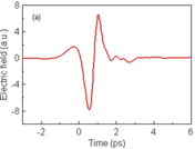
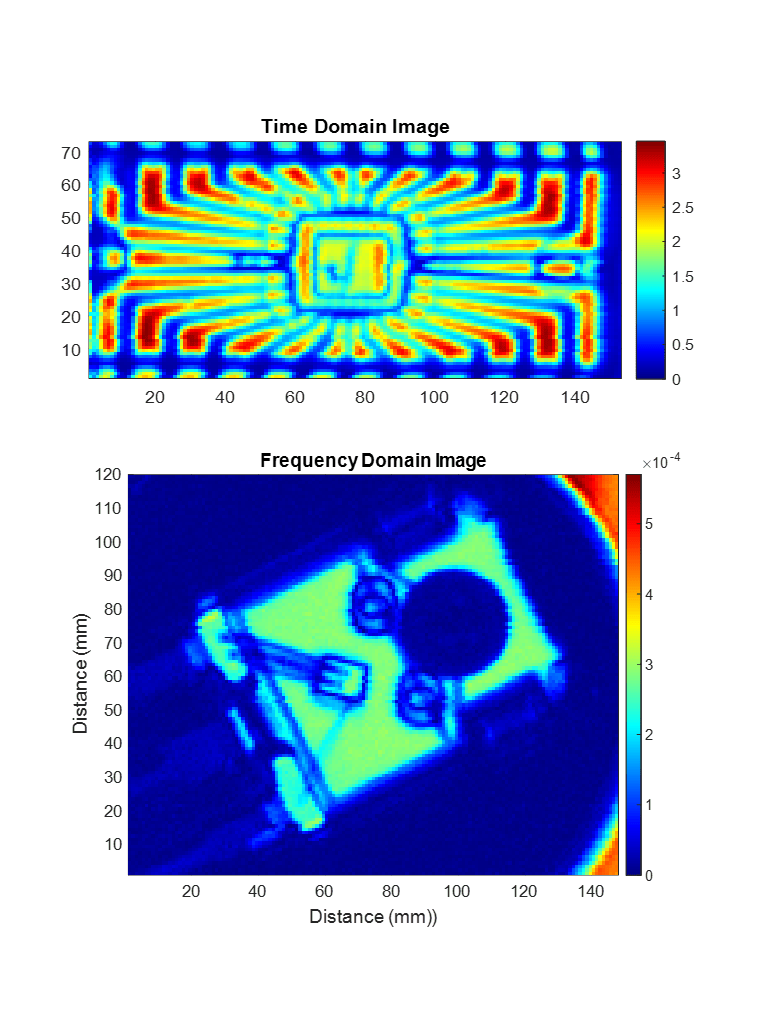
Once terahertz pulses were delivered to an array of spatial locations within the depth of packaged integrated circuits, the intensity of the reflected pulse at every point was used to recreate time domain images. Fourier transforms were performed on each pixel’s time domain signal to cut out lower frequencies and enhance image resolution.

Conclusions
-
The Terahertz Gap is a band of the electromagnetic spectrum that, when used for imaging, provides higher spatial resolution and contrast than the microwave band while retaining the ability to penetrate and not ionize samples, unlike frequency bands at and above the visible spectrum.
-
Terahertz pulses were provided to Integrated Circuit devices with optically opaque packaging at an array of points at depth and the reflected signal was recorded. When the images were processed, it was found that the reaction of terahertz band radiation with interconnect, semiconductor, and packaging materials provided enough contrast to visualize device features.
