Photopatterned Noble Metal Functional Surfaces Via Galvanic Replacement Reaction on Cu2O Thin Films
Student: Blake D. Trickey
Major Professor: Dr. Robert Coridan
Research Area(s):
Conventional Materials & Processes
Nanoscience & Engineering
Background/Relevance
- Cuprous oxide is a semiconductor with a wide use of photovoltaic and photoelectrochemical applications due to small band gap, also strong for direct photoelectrodeposition.
- Traditional photolithography used in many applications, such as structured electrocatalysts for energy conversion and microelectronics, but inefficient and time sensitive.
Innovation
- A more direct way to photopattern structures being more time and cost effective.
- Determine resolution limit of patterning
Approach
- Construct Michelson Interferometer.
- Michelson Interferometer deemed incorrect, too unstable.
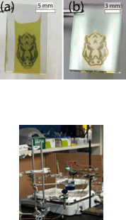
- Construct 1mm pinhole, 405 nm laser, 3 cm away, then pattern from circular diffraction.
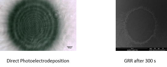
- Analyze patterning size of local changed chemistry of Cu nanoinclusions in Cu2O at solution temperature of 60°C.
- Use Galvanic replacement reaction to sacrifice Cu2O leaving behind Au.

Key Results
- Determined spacing around ~20 µm
- Galvanic replacement reaction washed away most of the pattern, leaving behind trace amounts of Au.
- Many of the patterns created exhibited a “blurred” pattern, as only 7/26 provided “clean” results.

Conclusions
- Patterning too intense in center from laser, too much Cu.
- Effective small patterning method confirmed by direct photoelectrodeposition.
- Future work desires to use a less intense laser to attempt to develop more Au.
- Future work dedicated to constructing a Lloyd’s mirror setup to pattern lines of patterned structures rather than the circular patterns.
