Structural Characteristics of Au-GaAs Nanostructures for Increased Plasmonic Enhancement
Student: Grant Abbey
Major Professor: Dr. Joseph B Herzog
Research Area(s):
Photonics
Background/Relevance
-
Free electrons in metallic structures receiving an incident electric field have been shown to exhibit collective oscillations and produce increased electromagnetic fields (i.e. plasmons).
-
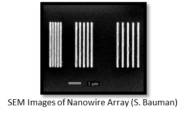
Deposition of metallic micro/nanostructures on a semiconducting substrate allow for generation of greater photocurrent in the device.
Innovation
- Enhanced structure design and accurate nanofabrication techniques will lead to greatly improved photovoltaic and photodetection applications.

Approach
- Generate Au/GaAs models in COMSOL FDTD software for nanoscale and microscale devices.
- Develop script in MATLAB to calculate and plot optical flux and photocurrent given raw data from COMSOL.
- Perform various parametric sweeps to vary structural aspects of the structure.
- Analyze and compare results to experimental data and publications involving similar structures.
Key Results
- Demonstrated computationally that a reduction in the gap between structures will generate an increase in optical enhancement due to plasmonic effects.
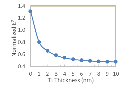
- Verified with experimental data that reduction of the thickness of both Au and Ti will generate more optical enhancement in the GaAs substrate.

Conclusions
-
Smaller nanogaps between structures increases the optical enhancement produced.
- Complete removal of the Ti layer significantly increases device performance.
- Decreasing the thickness of the Au layer increases photocurrent produced in the GaAs.

