
Growth of GePb & GeSn Alloy Films using Thermal Evaporator
Student: Hakimah Alahmed
Degree: M.S., December 2016
Major Professor: Dr. Hameed Naseem
Research Area(s):
Microelectronics
Photonics
Background/Relevance
- Crystalline Germanium plays important role in optoelectronic integration. However, incorporation of GePb or GeSn tunable(high hole and electron mobility) and more importantly direct band gap semiconductors. That suited very well with silicon platform based technology.
Innovation
- GeSn & GePb alloys have been used to get direct band-gap materials which are compatible with Silicon technology.
- GeSn is an ideal alloy, it can be use in high speed CMOS technology, co-integration of silicon compatible photonics and high performance transistor applications.
Approach
- Thermal evaporator is used for GePb and GeSn growth. Fig(4)
- Fisher Scientific muffle furnace used for GePb and GeSn annealing. Fig(5)
- The process schematic is shown below.

Key Results
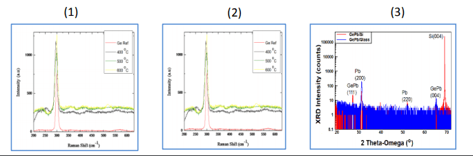
- Raman Spectra for GeSn at Different Annealing Temperatures (400-600 ºC). Fig(1).
- Raman Spectra for GePb at Different Annealing Temperatures (400-600 ºC). Fig(2).
- XRD Patterns for GePb/Si and GePb/Glass Annealed at 400ºC for 1 Hour Under N2 Environment. Fig(3).
Conclusions
- By using thermal evaporator GeSn and GePb layers have been deposited on silicon substrate, then they went through annealing process by fisher scientific furnace.
- HCl solution was used to etch GeSn and GePb samples.
- Raman spectra showed that the Ge-Ge peak shifted to left side, also the result give indication for incorporation of Pb and Sn in Ge.
- XRD results showed shifted in Ge peaks at (111) and (004) places and this refer to form of GePb
- The combination of lead and germanium led to lower annealing temperature required to crystallize germanium.
Future Work
- Growth of GeSn and Gepb on (Si & glass) substrate for different annealing time (15-30-60 min) and temperatures (400-600 °C) under N2 environment.