
Interfacial Contact with Noble Metal - Noble metal and Noble Metal – 2D Semiconductor Nanostructures Enhance Optical Activity
Student: Ricardo Romo
Degree: M.S., December 2019
Major Professor: Dr. Keith Roper
Research Area(s):
Photonics
Modeling & Simulation
Background/Relevance
- Nanoantenna-enhanced semiconductors exhibit extraordinary optical properties that allow nanoscale energy modulation (i.e. localized surface plasmon resonance (LSPR) and excitons.
- Applications such as optical switching, drug delivery, environmental sensors and photocatalysis can be derived from strong and weak coupling between plasmons and excitons in transition metal dichalcogenide (TMD)-heterostructures.
Innovation
-
Distinguishing respective contributions of plasmonic heating and hot electron transfer in noble metal – TMD heterostructures via experimentally and computationally.
Approach
- Produce TMD nanoflakes.
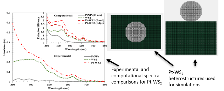
- Scanning transmission electron microscope (STEM) of the TMD-heterostructures.
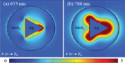
- Perform far- and near-field maps of the TMD-heterostructures via Discrete Dipole Approximation (DDA).
- Compare both computational and experimental optical feature enhancements.
Key Results
- Mapped local electric fields and hot electron transfer in 2D materials in order to distinguish relative thermal and hot electron transfer dissipation from LSPR.
- Distinguished respective contributions of electron transfer and plasmonic heating from DDA simulations.
Conclusions
-
These tools allowed comparison between the metal nanoantenna and the DDA simulations to determine relative contributions of plasmonic heating and hot electron transport to increase LSPR-enhanced photocatalysis from the TMD-heterostructure.
Future Work
-
Possible x-ray photoelectron spectroscopy (XPS), atomic force microscopy, and Raman spectroscopy to improve understanding of photoinduced doping of TMDs by metal nanoantennae.