
Characterization of Si-based GeSn Material and Devices for Short-Wave Infrared Applications
Student: Seyed Amir Ghetmiri
Degree: Ph.D., July 2016
Major Professors: Dr. Fisher Yu, Dr. Greg Salamo
Research Area(s):
Microelectronics
Background/Relevance
- Efficient optoelectronic devices for infrared wavelength beyond 2 μm is currently expensive.
- Monolithic integrated light sources on Si is needed for short-wave infrared applications
Innovation
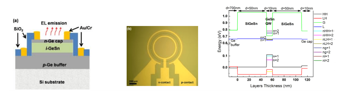
- Use CVD-grown direct bandgap GeSn material to fabricate large scale and cost-effective Si CMOS compatible light emitting diodes (LEDs).
- Simulate the bandgap energy of GeSn quantum wells and compare with GeSn QW emission from Photoluminescence (PL)
Approach
- Temperature-dependent PL on GeSn thin films with Sn composition up to 12%.
- I-V measurement, output power and Electroluminescence(EL) on the fabricated surface emitting and edge emitting GeSn DHS LEDs.
- Using MATLAB code to simulate the band alignment and quantized energy levels of the GeSn QW.
Key Results
- The GeSn thin films with different thicknesses and Sn compositions were grown using a commercially available CVD system.
- All samples examined under the PL measurement showed that the PL peak positions were shifted towards longer wavelengths once Sn composition increased.
- The GeSn films were changed to a TRUE direct bandgap material beyond a certain Sn composition and below a certain in-plane compressive strain.
- Double heterostructure (DHS) GeSn p-i-n LEDs (with 8 and 10% Sn) showed indirect bandgap emission behavior in different temperatures and low injection levels.
- The GeSn QWs with 10 nm thickness were grown between GeSn and SiGeSn barriers with lower Sn composition and examined under PL measurement.
- The PL intensity from the QW samples was higher and the peak position experienced a blue shift due to the confinement.
Conclusions
- High quality GeSn material is grown via commercial CVD technique.
- The high quality direct bandgap GeSn showed high intensity PL emissions in short-wave range of spectrum (between 2 to 3 μm).
- Better carrier confinement is needed to achieve a high intensity direct bandgap emission from GeSn LED.
- The studied GeSn QWs were indirect bandgap; however, SiGeSn as a barrier layer showed better confinement for GeSn QWs.
Future Work
- Using higher injection levels for the EL measurement of GeSn LEDs.
- More in-depth analysis of GeSn QW bandgap and compare with experimental results