
Monolithic GeSn Light-Emitter on Si for Integrated Photonic Circuits
Student: Yiyin Zhou
Degree: Ph.D., May 2020
Major Professor: Dr. Fisher Yu
Microelectronics
Photonics
Background/Relevance
- Si photonics plays great role in applications such as data communication and optical sensing.
- Efficient light-emitting source monolithically on Si is missing. Monolithic integration of light source on Si would make the Si photonics more cost-effective, compact, and reliable.
Innovation
- Low-cost light source on Si meets the need of light source integration for Si photonics.
- Tunable light emission wavelength from near- to mid-infrared enables a wide range of applications.
Approach
- Device simulation was performed by using MATLAB, TCAD, FDTD simulation software.
- Epitaxial growth using commercial RP-CVD under CMOS compatible temperatures.
- Material characterization using techniques such as PL, Raman, Ellipsometry, XRD, SIMS, TEM, and etc.
- LED and laser devices fabrication using standard fabrication process.
- Device was tested at cryogenic temperatures.

Key Results
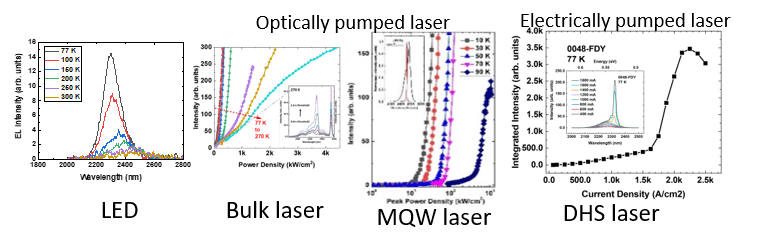
- On Si direct band gap GeSn LEDs were achieved with peak power of ~ 50 µW.
- Optical pumped GeSn bulk Laser was achieved at 270 K.
- Optical pumped multiple quantum laser was studied with low threshold at 25 kW/cm2.
- Electrically pumped GeSn laser has been firstly demonstrated!
Conclusions
- Material characterizations resolves the information strain, band gap energy, and defect density.
- Optically pumped lasers was demonstrated with a near room-temperature operation and reduced threshold at low temperature.
- LED designs enables the study the diode device performance.
- Electrically pumped lasers were demonstrated with maximum temperature potation at 100 K and threshold density of ~3kA/cm2.
Future Work
-
Optimize the device structures for higher performance in efficiency and maximum operating temperature.