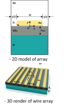
Dataset for SERS Plasmonic Array: Width, Spacing, and Thin Film Oxide thickness optimization
Student: Chris Klenke
Major Professor: Dr. Joseph Herzog
Research Area(s):
Modeling and Simulation
Photonics
Background/Relevance
- Previously, Dr. Herzog and his research group have published several works regarding plasmonics in Au nanostructures.
- Other researchers have published computational work that should yield similar results but have gotten discrepancies.
Innovation
- Publish our data and methods in the open-access MDPI Journal DATA to allow other researchers to verify and validate our work.
- Make our data available in a universal format that can be tested with computer modeling software other than COMSOL, such as MATLAB
Approach
- Computationally model an array of Au nanowires on an SiO2 substrate with various parameters.
- Perform with COMSOL, a physics modelling software using finite element method (FEM).
- Vary the widths of the nanowires (w), the spacings between the wires (s), and the depths of the SiO2 (tSiO2) and analyze plasmonic enhancement for each variation
- Export data into plaintext text files to make accessible to researchers without COMSOL.

Key Results
- Differing values of s and w at the nanoscale provide varying degrees of plasmonic enhancement.
- There exist parameter combinations that provide strong plasmonic enhancement at values previously unstudied.
- Periodic values of tSiO2 provide periodic amounts of plasmonic enhancement, apparently irrelevant to the rest of the structure.

Conclusions
- Stronger than expected plasmonic interference occurs in nanowires spaced greater than 100 nm apart, an area of plasmonics that has not been investigated much.
- This can possibly be utilized for creating substrates for surface-enhanced Raman Spectroscopy (SERS).
- The data can be evaluated in other modelling softwares to allow for accurate validation by fellow computational modelling researchers.
